
Cambridge 7th to 9th September

Presenting Author:
Suraya Kamil
<pmsakh@leeds.ac.uk>
article posted 01 Apr 2015
Suraya Ahmad Kamil (pmsakh@leeds.ac.uk)
Suraya is originally from Malaysia and currently a PhD student at the University of Leeds,
working with Prof Gin Jose. She received her Bachelor Degree in Applied Physics from
University Malaya and Master's Degree in Physics from Universiti Sains Malaysia.
Her research is focused at developing functional photonic layer on silicon platform by
forming glassy layers using laser plasma processing.
Implantation of erbium doped TeO2-ZnO-Na2O glass into silicon for gain media in silicon photonics
Matthew Murray1, Suraya Ahmad Kamil1*, Stuart Micklethwaite1, Tim Nunney2, Jon Treacy2, Gin Jose1
Silicon photonics represents a technological solution to the industrial and societal challenge of increasing internet speeds and capacity, without burdening the financial and power dependencies of networked systems [1]. A key example of this is traditional copper wiring used in datacentres both increasing cost and decreasing communication speeds, which a combined fibre optic and silicon photonic system could dramatically outperform [2].
These challenges are growing and the need for valid solutions increasingly apparent, however silicon photonics still lacks key developmental components in this upcoming revolution in data communications architecture. One such component is integrated gain media, brought about due to the fundamental limitations of silicon (indirect bandgap, low doping solubilities of optically active ions, etc.).
We present a novel CMOS compatible surface processing route, termed ultrafast laser plasma implantation (ULPI) [3], to grow a highly rare earth doped glass layer upon the surface of silicon, thus serving as a possible solution to dramatically increase gain in future devices. Tellurite zinc sodium glass targets doped with Er3+-ions are ablated with a femtosecond laser and implanted into single crystalline silicon substrates heated to 570°C.
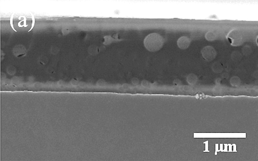 Rapid quenching of the implanted material
has been found to encourage the formation of a metastable glassy layer atop silicon,
with a very well defined interface to the pristine Si substrate, unique to the ULPI process
and shown in
Rapid quenching of the implanted material
has been found to encourage the formation of a metastable glassy layer atop silicon,
with a very well defined interface to the pristine Si substrate, unique to the ULPI process
and shown in Figure 1(a).
Fig 1(a) Cross-sectional SEM image of Er:TZN implanted Si
XPS was used to probe the homogeneity and composition
of the implanted layer, showing a highly refined mixture of silicate and tellurite glass
phases and Er concentration of 2.0 at%.
 This process can be further optimised to inhibit
the formation of any particulates in the film, forming a highly-dense rare earth doped
region within a silicon photonics platform to serve as a gain medium. This too would
enhance the lifetime and fluorescence qualities shown in
This process can be further optimised to inhibit
the formation of any particulates in the film, forming a highly-dense rare earth doped
region within a silicon photonics platform to serve as a gain medium. This too would
enhance the lifetime and fluorescence qualities shown in
Figure 1(b)
for Er3+ ions.
Fig 1(b) Room temperature (RT) Er3+: 4I13/2 --> 4I15/2
photoluminescence (PL),
 Furthermore, shadow masking can be employed to deploy these regions with micro-scale
dimensionality, ideal for silicon photonics.
Furthermore, shadow masking can be employed to deploy these regions with micro-scale
dimensionality, ideal for silicon photonics.
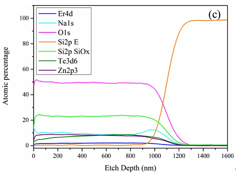
Fig 1 (c) depth resolved XPS analysis of Er:TZN implanted crystalline silicon
References:
[1] J Doylend et al, The evolution of silicon photonics as an enabling technology for optical interconnection, Laser and Photonics Reviews, 6, 504-25 (2012)
[2] A. Rickman, The Commercialization of silicon photonics, Nature Photonics, 8, 579-82 (2014)
[3] http://www.google.com/patents/WO2013117941A3?cl=en