
Cambridge 7th to 9th September
Presenting Author:
Vinita Mittal
article posted 17 June 2015
Vinita Mittal
Vinita Mittal is currently a third year PhD (Photonics) student at the Optoelectronics Research Centre, University of Southampton, UK. Her research focuses on the fabrication of integrated photonic devices using novel materials for the mid-infrared region, for biomedical diagnostic applications. She is working in chalcogenide materials to develop waveguide-based biosensors. Her interests lie in material synthesis, thin film technology and the structural and optical characterisation techniques. She is an active member of OSA and SPIE, University of Southampton student chapter and also holds Social officer position in the chapter. She received her Master of Technology degree in Materials Science and Engineering from the Indian Institute of Technology, Kharagpur, India in 2012.
.
High contrast mid-infrared chalcogenide waveguides for biosensing applications
Vinita Mittal, James S Wilkinson and Ganapathy Senthil Murugan
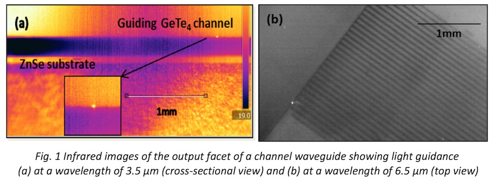
Mid-infrared spectral band from 2 μm – 20 µm is ideal for label-free biosensing as the fundamental vibrations of many significant biomolecules take place in this region. Mid-infrared absorption spectroscopy using FTIR has been exploited for the last few decades to provide sensing capabilities for biomedical diagnostics. However, the sensitivity and the detection limit of the sample under test can be tremendously improved by using the evanescent field based integrated planar waveguide devices. In this paper, we present the fabrication and characterization results of chalcogenide waveguides transparent in the mid-infrared region for such applications. GeTe4 waveguides on ZnSe substrates were fabricated using lift-off technique. Lift-off resist was used to create the patterns on ZnSe substrate using photolithography and GeTe4 was deposited on these patterned samples using RF sputtering. The lift-off resist was stripped off to obtain the desired channels. The waveguides were characterized in both mid wave (2.5 µm – 3.7 µm) and long wave (6.4 µm – 7.5 µm) spectral bands using optical parametric oscillator-based laser source and quantum cascade laser, respectively [1]. Fig. 1 (a) and (b) show the cross-section and top view of the infrared camera images of the output facet of a GeTe4 channel waveguide showing light guidance at λ = 3.5 µm and λ = 6.5 µm, respectively.
ZnSe used as a substrate is a soft polycrystalline material and it was difficult to polish the end-facets of the samples using conventional polishing without chipping. An alternative approach of depositing both lower cladding (isolation layer) and core material of the waveguides on Si substrate was employed to utilize the well-known cleaving planes of Si to avoid polishing. Silicon is also a cheaper and convenient substrate. Here, thickness of ZnSe (n ~ 2.4), which is the isolation layer between the high refractive index Si substrate (n ~ 3.5) and the core of the waveguide (GeTe4, n ~ 3.3) was calculated by numerical modelling so that the propagating mode does not get affected by the underneath high refractive index Si substrate. ZnSe was deposited using thermal evaporation on Si and was annealed to release the thermal stresses in the film and to increase its adhesion. GeTe4 waveguides were then fabricated on top of ZnSe/Si using lift-off technique. The end-facet of the sample was cleaved for coupling the light into the waveguides and the waveguides were characterised in the mid-infrared region.
Acknowledgement:
This research is funded by the European Research Council under the EU 7th Framework Programme (FP7/2007-2013) / ERC grant agreement no. 291216.
References:
[1] V. Mittal, A. Aghajani, L. G. Carpenter, J. C. Gates, J. Butement, P. G. R. Smith, J. S. Wilkinson, and G. S. Murugan, Opt. Lett. 40, 2016-2019 (2015).